Gate-and-switch-level modeling
本文最后更新于:Wednesday, September 30th 2020, 8:02 pm
Gate-and-switch-level modeling
1、verilog-std-1364-20051
There are
14 logic gatesand12 switchespredefined in the Verilog HDL to provide the gate- and switch-level modeling facility. Modeling with logic gates and switches has the following advantages:
— Gates provide a much closer one-to-one mapping between the actual circuit and the model.
— There is no continuous assignment equivalent to the bidirectional transfer gate.
Verilog1364-2005标准规定了26个基本原件,其中14个门级原件,12个开关级原件。
对于这些原件不需要定义直接调用。
2、门级建模2
多输入门:
1
2
3
4
5
6
n_input_gate_instance ::= [ name_of_gate_instance ]
( output_terminal , input_terminal { , input_terminal } )
and A1(out1, in1, in2);
or O1(outa, inb, inc, ind);
xor X1(outx, inx, iny, inz, inw);多输出门调用:
1
2
3
4
5
n_output_gate_instance ::= [ name_of_gate_instance ]
( output_terminal { , output_terminal } , input_terminal )
buf BUF_1(bufout1, bufout2, bufout3, bufin);
not NOT_1(out1, out2, in);三态门调用:
1
2
3
4
enable_gate_instance ::= [ name_of_gate_instance ]
( output_terminal , input_terminal , enable_terminal )
bufif1 BF1(data_bus, data, enable);二个电阻
The instance declaration of a pullup or a pulldown source shall begin with one of the following keywords:
pullup,pulldown1
2
3
4
5pull_gate_instance ::= [ name_of_gate_instance ] ( output_terminal )
pullup (strong1) p1 (neta), p2 (netb);
In this example, the p1 instance drives neta and the p2 instance drives netb with strong strength.注意: 门级原件的端口列表都固定好了,可以不用定义中间连接信号类型(wire)
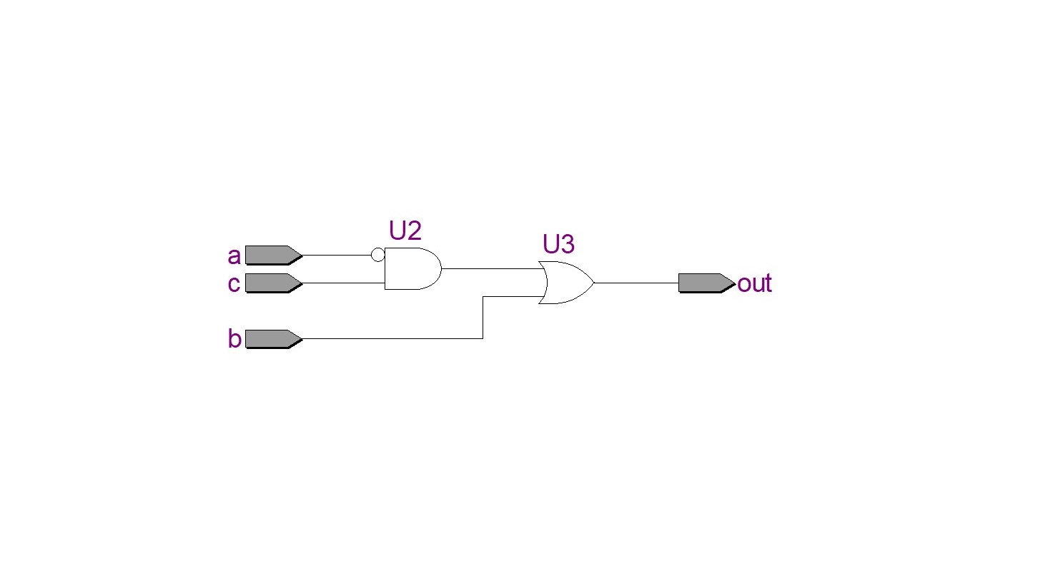
示例:
1 | |
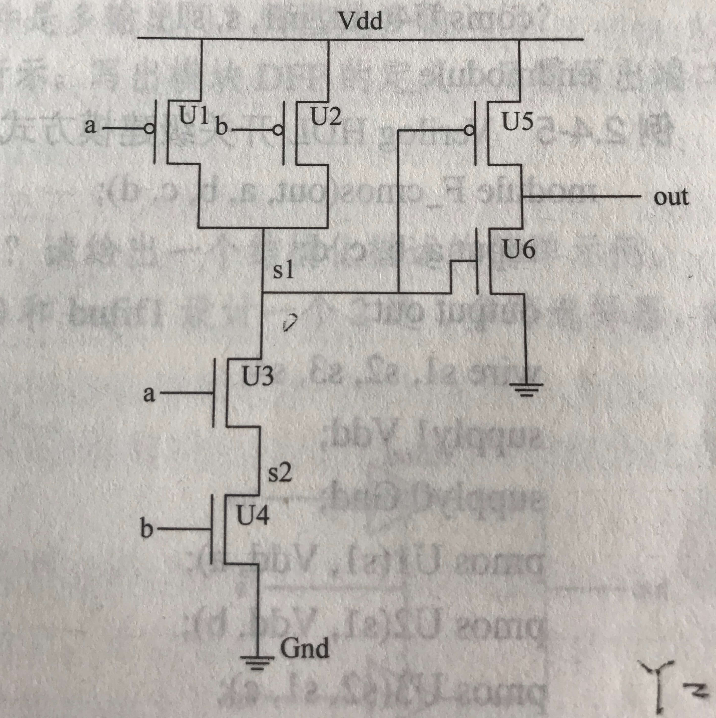
3、开关级建模
- MOS switches
| cmos | pmos | nmos |
|---|---|---|
| rcmos | rnmos | rpmos |
rmos : 代表晶体管导通时源漏有较高的阻抗(
impedance)
1 | |
- Bidirectional pass switches(双向开关)
| tran | tranif1 | tranif0 |
|---|---|---|
| rtran | rtranif1 | rtranif0 |
The bidirectional pass switches shall not delay signals propagating through them. When tranif0, tranif1,rtranif0, or rtranif1 devices are turned off, they shall block signals; and when they are turned on, they shall pass signals. The tran and rtran devices cannot be turned off, and they shall always pass signals.(双向开关没有传播延时)
1
2
3
4
5
The following example declares an instance of tranif1:

tranif1  t1 (inout1,inout2,control);

The bidirectional terminals are  inout1  and  inout2 . The control input is  control . The instance name is t1 .
1 | |
示例:
1 | |
quarter II 综合不了,没办法直接看viewer。只能把书上的图扒来了。
终于找到了一款RTL级,gate级,开关级debugger和viewer的软件
trainsistor-level debugger and viewer
但是目前下载不了,得找客服联系。不知有人有用过这款软件没有。有的话请你一定告诉我。
Renference
本博客所有文章除特别声明外,均采用 CC BY-SA 3.0协议 。转载请注明出处!